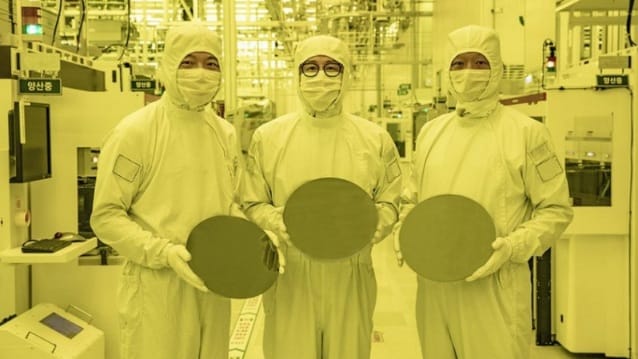
SAMSUNG Starts Production of Chips With 3-Nanometer Technology, Faster and Sophisticated!
Table of Contents
Samsung Electronics Co., Ltd announced that it has started mass production of advanced chips. The chip has 3-Nanometer (nm) technology that implements the Gate-All-Around (GAA) transistor architecture.
This first GAA technology has several advantages. Such as reducing power consumption, while increasing performance. Nanosheet technology is claimed to have higher performance and greater energy efficiency.
By leveraging the 3nm GAA technology, Samsung will adjust the channel width of the nanosheet. The goal is to optimize the use of power and performance tailored to the needs of customers.
According to Samsung, compared to 5nm chips, the first generation 3nm chips are more efficient at reducing power consumption by 45%, increasing performance by 23% and reducing area by 16%. While at 3nm the second generation can reduce power consumption by up to 50%, increase performance by 30% and reduce area by up to 35%.
“Samsung has grown rapidly as we continue to demonstrate leadership in implementing next-generation technologies for manufacturing, such as High-K Metal Gate, FinFET and EUV. We seek to continue this leadership with the world's first 3nm process with MBCFET,” said Dr. Siyoung Choi, President and Head of Foundry Business at Samsung Electronics.
"We will continue to actively innovate in the development of competitive and constructive technologies to accelerate the achievement of technological developments." he added.
Chip manufacturing with this advanced technology is expected to bring more Samsung customers looking for innovative and powerful semiconductors. As well as enabling technology products more quickly and efficiently. (*)
Photo: News Samsung


Post a Comment